PCB milling with a CNC 3018
What I learned about milling PCBs with a cheap CNC 3018 to build a guitar amplifier.

Why do I want to mill a PCB?
Nowadays, ordering professionally made PCBs is very cheap and easy in websites like PCBWay or JLCPCB, so typically you won’t need to build your own PCBs to build your own circuits. However, milling your own PCBs is somehow satisfactory when it works well(⚠️), and it is a good starting point for learning more generic CNC skills. I took it as a learning exercise.
⚠️: The iterations needed to get it working well can be quite frustrating though. My experience was: getting a decent PCB after 4~5 tries, getting one crappy PCB afterwards, touching here and there, iterating a few ~3 times, getting a nice PCB, not understanding why next PCB is not ok, etc. Spending PCBs, mills, and mostly time. But I felt challenged to understand what was going wrong in the process, so I could not stop until I got something decent.
The more I practice, the more I understand all aspects that can go wrong. Note that most of my issues came from the fact that my setup is cheap, but I would need a very good excuse to buy a more expensive setup.
My setup
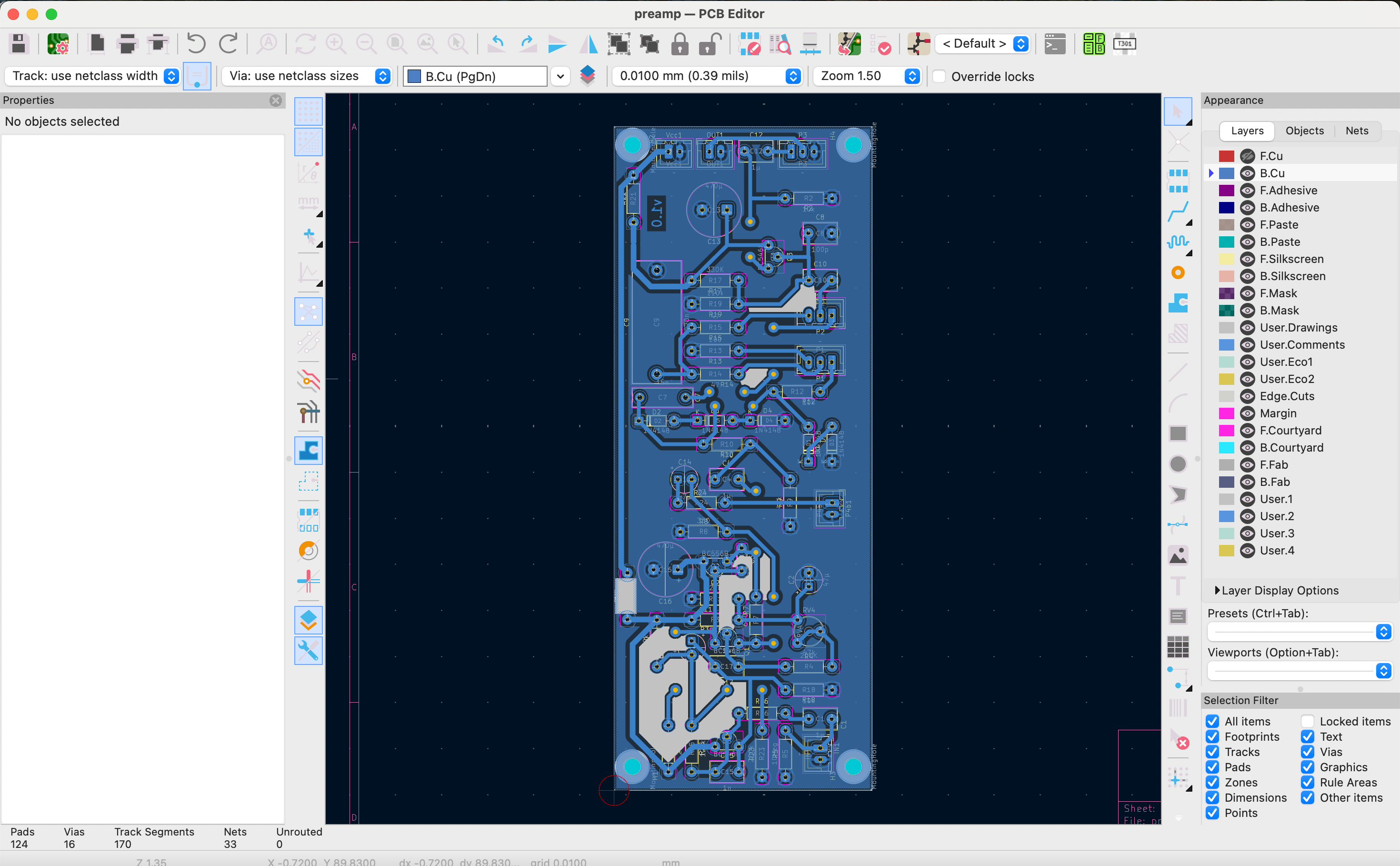
PCB design: Kicad
I’ve only built PCBs with very generous track and clearance widths, to make things easier, since my design is a simple guitar amplifier without digital components. I used a default 0.5mm minimum clearance between tracks, and 0.8mm minimum track width. Pending to experiment with more challenging designs, e.g. digital designs with thinner tracks and clearances.
GCode generation: EasyTrace5000
Once I had the gerber files, I had to generate gcodes for my CNC machine. In 2026, I think the most easy way to do it is with https://cam.eltryus.design/easytrace5000/. It is not a hell to make it work as FlatCAM, it is not as limited as Carbide Copper, it is more friendly than pcb2gcode, it is free unlike CopperCAM, etc.
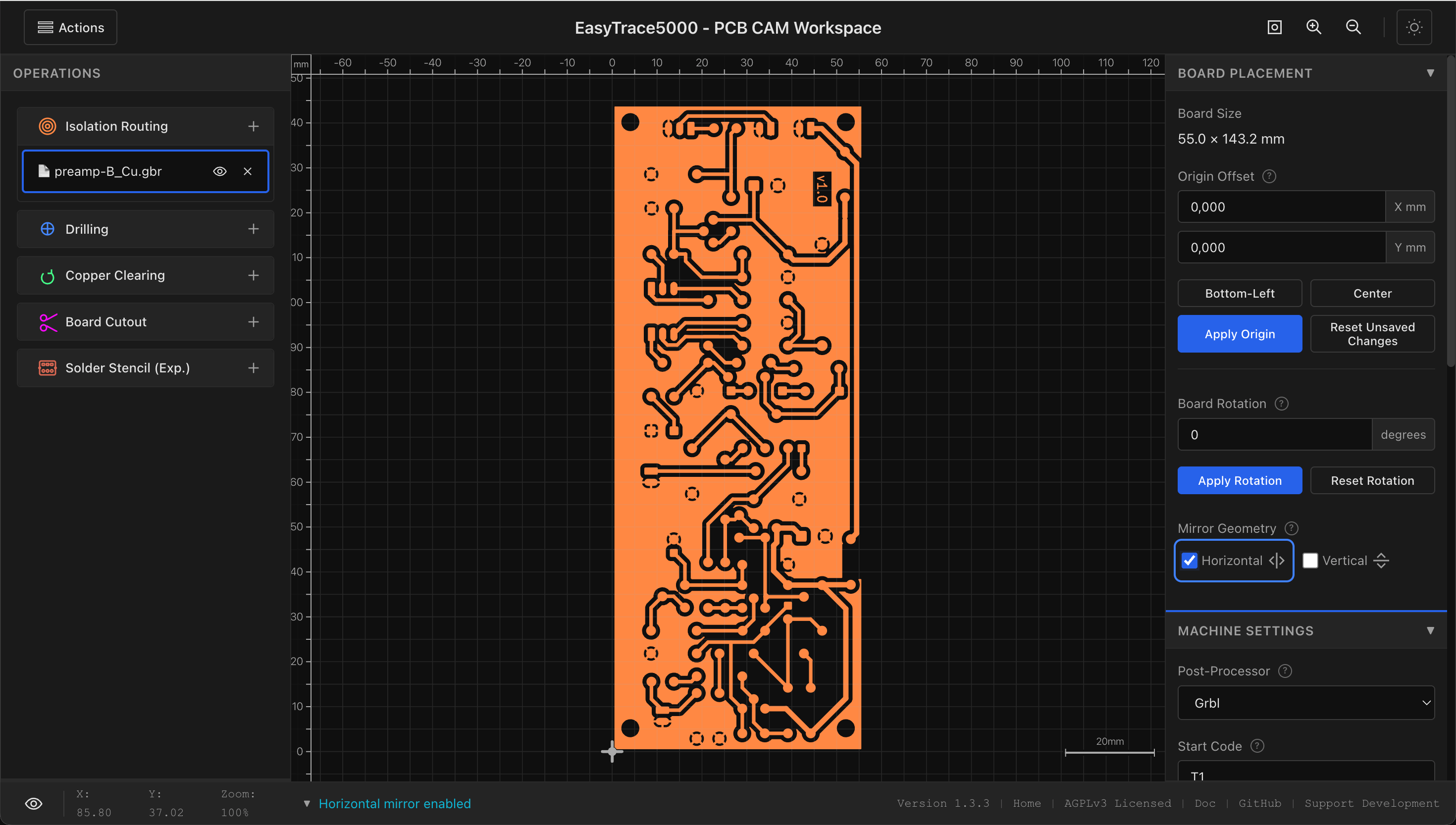
Note that you should mirror your PCB for milling the bottom layer, something that is not automatically done in gerber files. If you add some text in the layer, you will notice easily if it can be read or it is reversed. Note: my first PCB was not mirrored.
The configuration parameters that worked for me:
You should select a tool diameter slightly bigger (0.02~0.05mm) than the actual size of your mill, since your cheap CNC will probably have some radial runout in the movement of the mill. About the number of passes, in my experience 3 is enough if the rest of parameters is enough. About Z cut-depth, 40µm (-0.04mm) is the minimum limit. I would suggest that you first try with this value, and if it is too low, you can increase it later easily. The plunge rate in my case was 20, feed rate 100, spindle speed 10000rpm, dwell 1.
Sending Gcodes to the CNC: Universal GCode Sender
I think Universal Gcode Sender is a very nice way to communicate with your CNC. I learned how to use the tool with the help of GPT very easily, so I won’t explain how to do it.
Autoleveler
The success in PCB creation is about having your bit milling exactly the thin 35µm (0.035mm) of copper of a standard PCB, and nothing else. Of course, this micrometric precision in Z-axis is quite hard to achieve with such a crappy equipment.
Too deep: If you deepen too much in Z-axis, the milling is going to be quite horrible for a variety of reasons: the V-bit widens as you go deeper in Z, the cut is not happening in the tip but in the cone, the copper deforms before it is sheared so it creates burrs, the amount of material to be removed increases and it is mechanically more challenging leading to imprecision… Even a 0.02mm extra deep can be noticeable in this aspect.
Too shallow: If you do not go deep enough, you just leave the copper there, so your PCB won’t work.
If you go e.g. ~0.02mm too deep, or too shallow, you might be failing in your PCB creation. This is the real pain.
Also PCBs are not perfectly flat, especially when placed in the surface of your CNC, so variations of >~0.10mm in height are frequent: of course, this is a non-go for PCB milling. If, for some reason, you do not compensate this properly, you might get something like this:
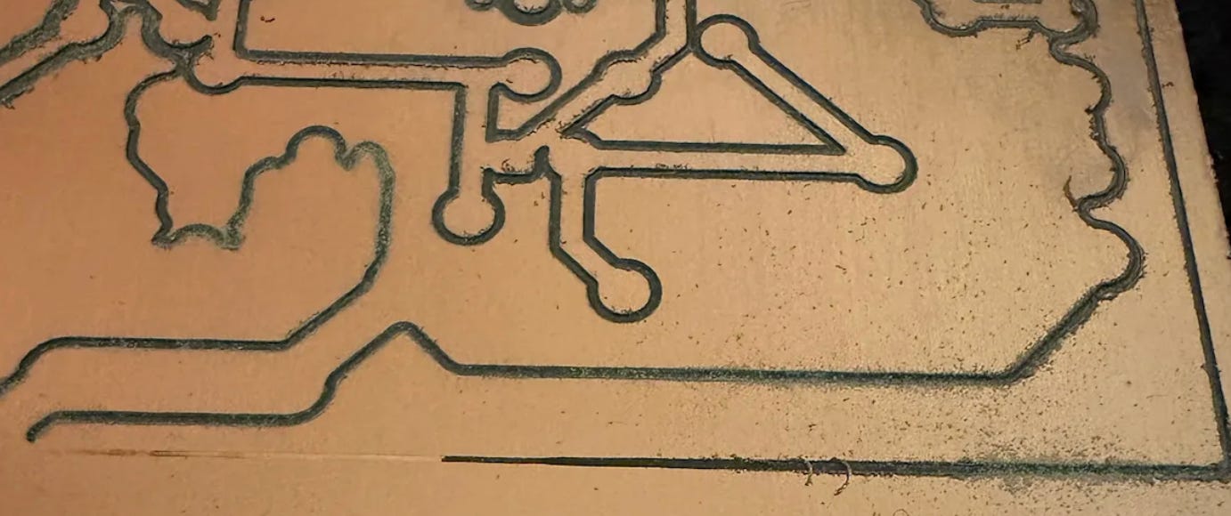
In the left side, it didn’t mill the copper, and in the right side it milled too much (you can even see some burrs, etc).
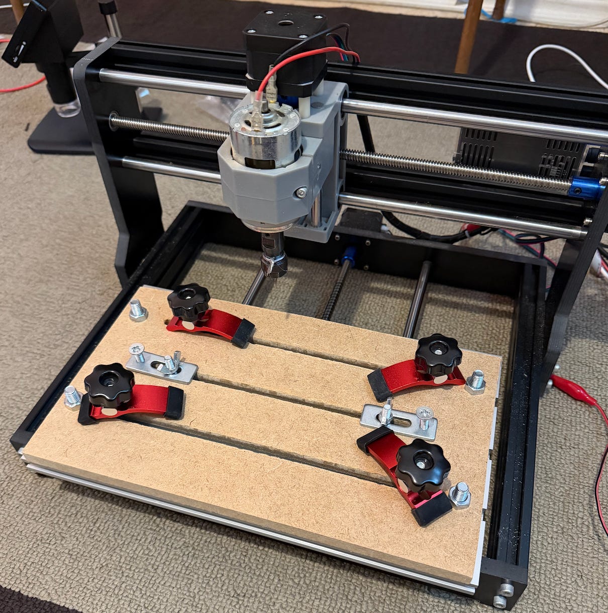
Due to that, UGS has a “autoleveler” plugin that is very convenient: it uses the “probe” connection of the CNC to detect when there is electric continuity between your mill and the copper. Of course, you have to connect a cable to the mill (I used a bare cable in the metallic part of the drill with a crocodile clip), and a cable to the PCB. See in my picture how I did it.
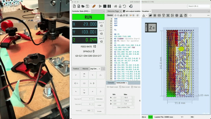
It is then able to create a heights-map able to compensate that the PCB is not perfectly flat. In my case, I got good results with a resolution of 1cm in the autoleveling.
CNC 3018
My CNC is a SainSmart Genmitsu CNC 3018-PRO with working area 300x180x45mm. I bought in AliExpress long time ago for less than 200€. I can’t find anymore this exact model, but the offer is huge.
It is a cheap machine: not very rigid, not very powerful, etc. but should be enough to create PCBs.
Flattened sacrificial wood
I cut a sacrificial wood of MDF with some strips to place the clamps. It took a while, but I wouldn’t really know how to proceed without it. In the picture I show it is not done yet, but I also flattened to z = -1mm a big surface using the biggest flat mill I had. This helped a bit to compensate a systematic tilt it had.
Bare board PCB
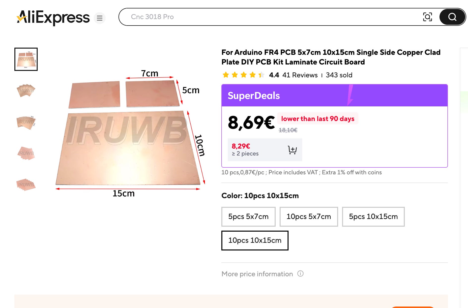
I bought cheap PCBs in AliExpress. I only used phenolic boards (FR1/FR2), just to extend the lifespan of my mills. Maybe FR4 (glass fiber) is better in terms of flatness, I am not totally sure.
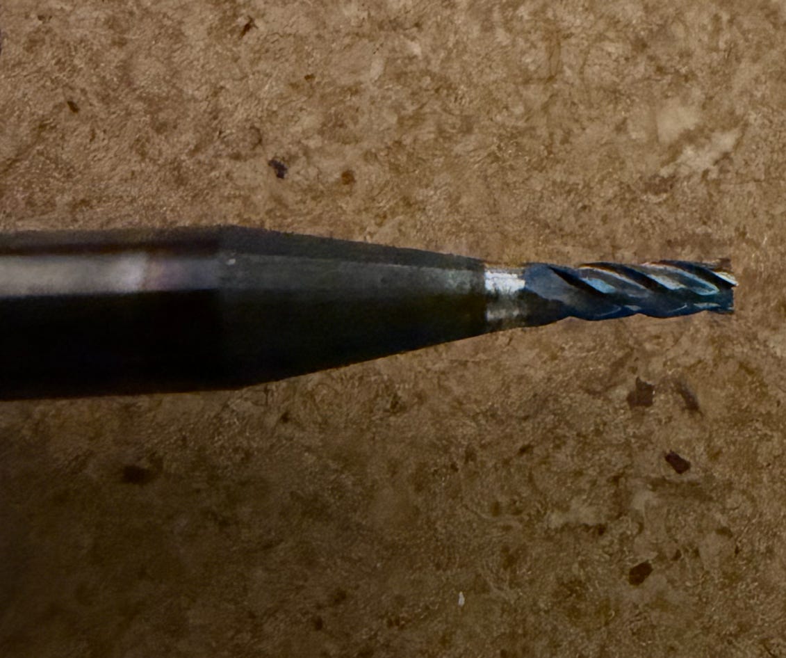
Mills
I’ve been using V-bit mills, because 0.1~0.2mm flat mills are too fragile for the vibrations of a CNC 3018.
Initially I started with 0.1mm / 20º mills, but I realized they are quite fragile too. Sometimes, if the Z-depth was not very well set, they didn’t last more than one PCB.
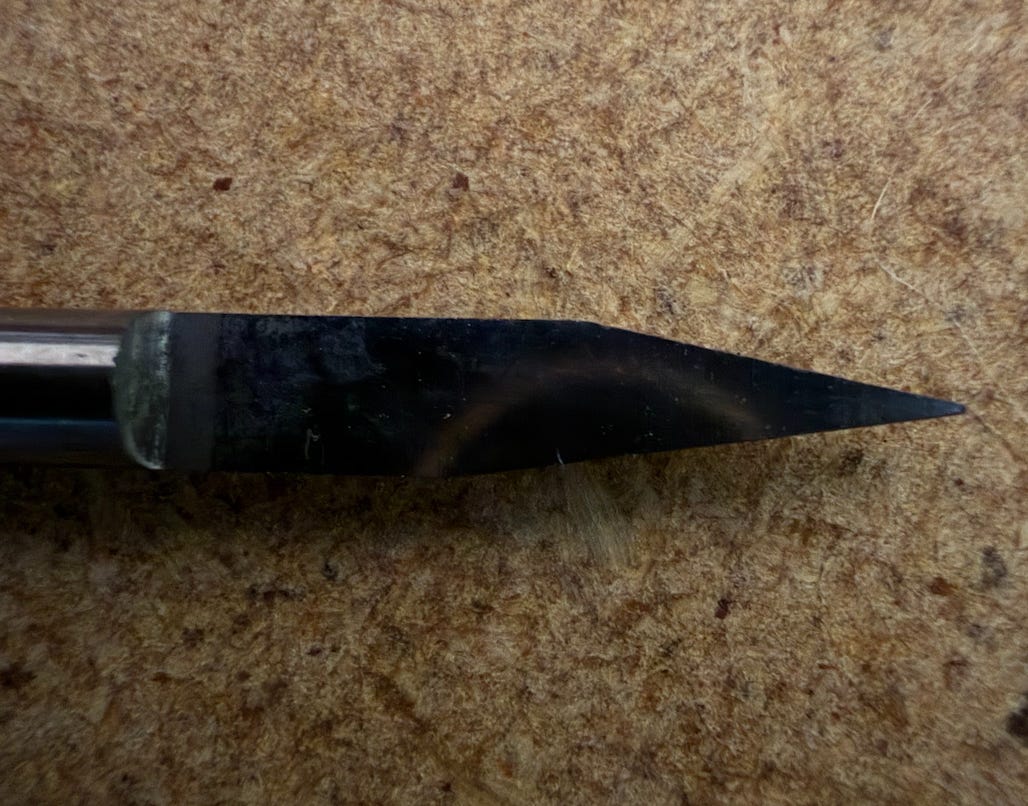
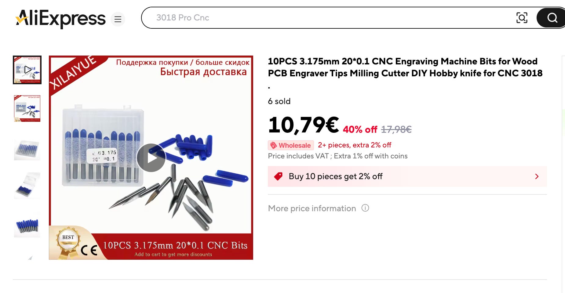
Then I switched to V-bit pyramidal 0.2mm / 30º: they look definitely stronger, and it seems a bit harder to damage.
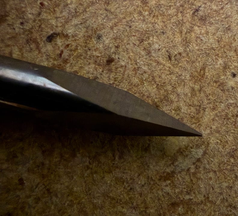
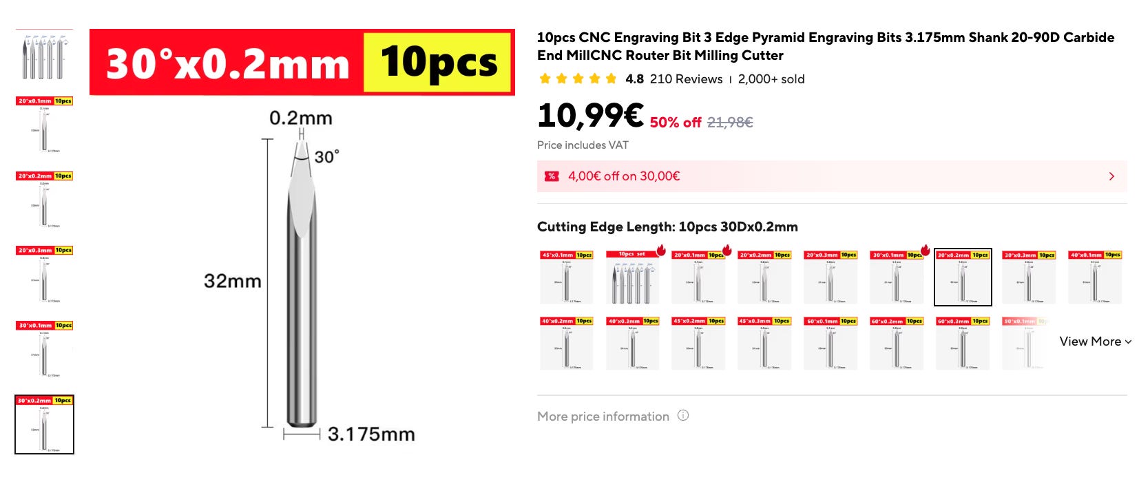
I got good results with this one, so it is the one I am using now. After all, 0.2mm is thin enough for most purposes.
I also have a carbide 4-flutes 1.5mm flat mill for edge cuts and copper clearing:

Gallery
Some examples of my successes and failures:
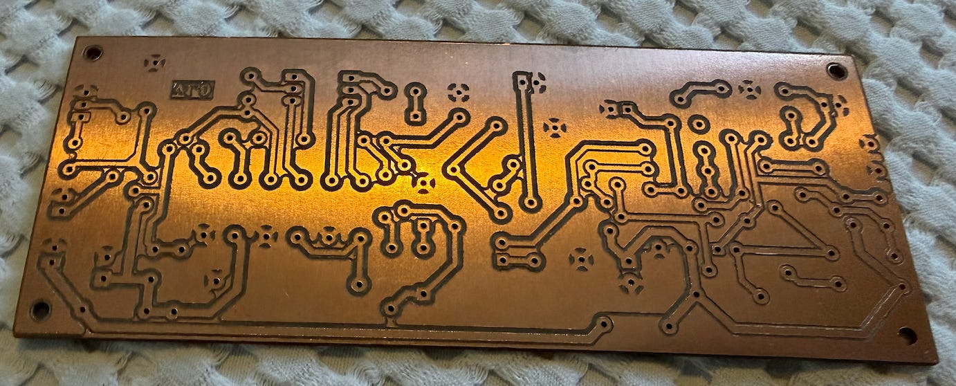
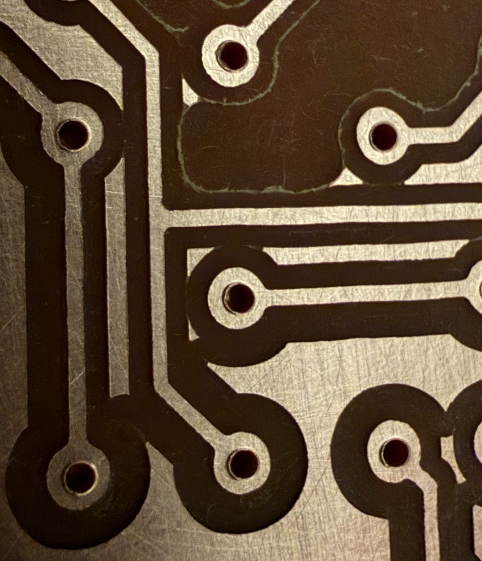
A decent PCB:
Which looks good if you look closer.
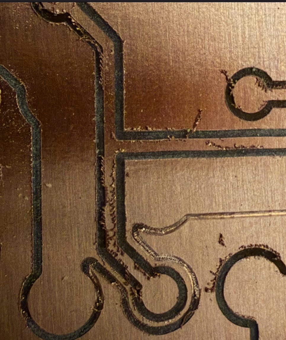
But it wasn’t always like that…
This happened due to missed steps in Z-axis in the stepper motor of the CNC:
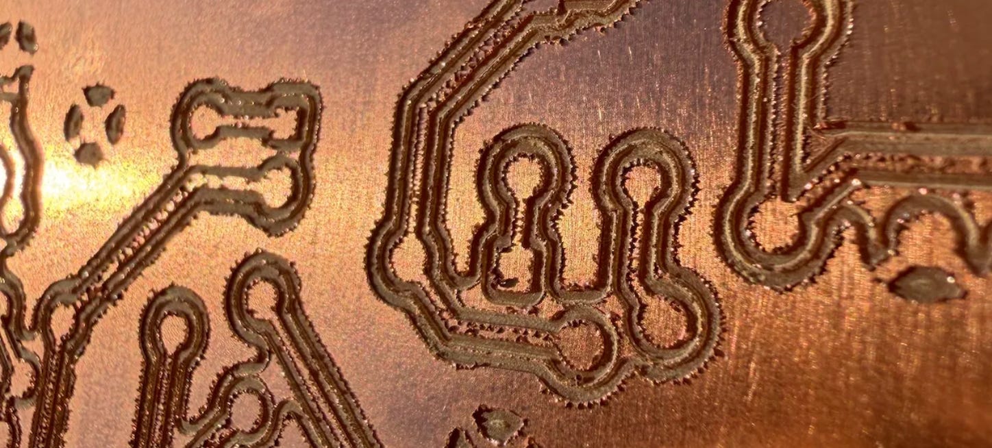
And this one happened because of a slightly damaged mill:
Checklist of considerations
Here I collect a list of things that can go wrong, in my experience, for PCB milling. I sort them according to their importance.
You are missing steps in your stepper motors: For example, the CNC axes are not properly lubricated, or the speeds and accelerations being used are too high. This causes skipped steps, which makes it completely impossible to create the PCB. This is especially delicate for the Z-axis, where you need <0.01mm precision, so I run $112=200 (capping the maximum speed to 300 mm/min) and $122=10 (limiting acceleration to 10 mm/sec²) in advance to ensure the motor doesn’t stall. Using the Z-probe you can check the extend of the issue, by checking if the probe activates at z=0.00mm in the same point after some time. This was a headache in my case.
The screws of the machine are not tightened: it might produce vibration and contributing to many other issues.
The mill is slightly damaged: you should use a lens or microscope to check the status of it. Sometimes, just a close inspection with some magnifier lens makes clear it is broken, but in some other times it is not easy to know if your mill is not in perfect shape. The feeling with pinching your skin or nail is quite indicative sometimes too of sharpness. Be aware of the “history” of your mill: if you did some milling with issues in the past, maybe the mill might be damaged. If you are having issues with some PCB, you can try a different mill, and if everything goes well now, you found the issue and you can discard the previous mill. In my experience, 0.1mm / 20º V-bit mills are quite more fragile than 0.2mm / 30º, so I am now using the second ones.
Your milling parameters are not correct. I recommend z-cut of 0.04mm at the beginning (you can increase it without regenerating the gcode file, just by changing the place of the z=0.00mm in UGS). Use feed rate of 100, plunge rate of 20. About the number of passes, 3 should be enough.
Autoleveling was run, but then you touched something in UGS software: you must be very careful about not touching any number once the autolevel is done: when it finishes, just removes the clips and launch the gcode file.
PCB is not properly clamped, or it is clamped with too much pressure so it is curved. It should look visually flat. The autolevel, in theory, compensates this, but I would try to have it as flat as possible from the beginning. If you sacrificial board is tilted, you can mill a large surface a z=-1mm, so that it is perfectly aligned with your CNC.
PCB can be flexed easily when touched. The mill might flex the PCB during the process and the Z-depth might be wrong. I use plunge rate of 20 just in case this is happening in the center of a clamped big PCB, but if you case it is very noticeable, you can use masking tape with superglue in both surfaces (your PCB and your sacrificial wood), without overlap between the tapes. Search about this trick on internet. This point, anyway, wasn’t very important in my case, using a plunge rate of 20.
Autoleveler had not enough resolution: in some cases, I had the feeling that less than 10mm was better in this aspect, but I have no prove of it.
Drilling & Edge cutting
Drilling is a much easier aspect to handle for me than milling, so I won’t talk much about this point. The only consideration with EasyTrace5000 is that, given that you are mirroring your PCB design, you need to mirror the drills (exported by KiCad) too. And EasyTrace5000 mirrors using as center axes the medium point between the most left point and the most right one. This might produce a different mirroring axis than in the case of the PCB.
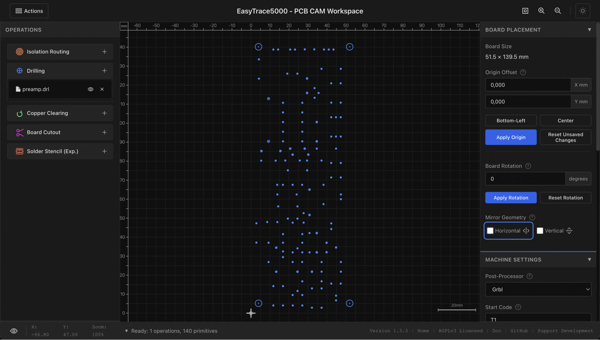
So I suggest to put together then PTH and NPTH drill holes, and make sure that the mirroring axis falls exactly in the middle of the PCB. This will happen if the mounting holes are in the extremes, with same distance to the end of the board. Then, when you mill your PCB using UGS, just do not change the X and Y coordinates references, replace the mill by a drill (I use 0.9mm), adjust Z-height more or less, and launch it.
For the case of edge cutting, I use the 1.5mm carbide flat mill, because the operation is quite more aggressive than isolation routing, but EasyTrace5000 and UGS is very easy to manage for this operation.
Cleaning your PCB
Even if your PCB process was right, you need to clean it to remove burrs. In my case that was easy: just gently wash it with soap an a scrub sponge as you do for a dish. I got good results with this, no sign of burrs or whiskers, and the copper was just very slightly scratched (I consider it acceptable).
